Post
Extreme Ultraviolet Lithography
EUV lithography is the near-impossible machine that turned atomic-scale physics into a manufacturable process, keeping Moore’s Law alive when everything else failed.
The new-generation chips that you see today, a single chip can contain billions of transistors.
That means:
Billions of tiny switches… On something smaller than a fingernail… Working reliably, at insane speeds.
That got me thinking: how do they even fit so much, with such precision, and make it actually work?
The answer: A fascinating rabbit hole called EUV Lithography often called “the machine that saved Moore’s Law.”
The Core Problem
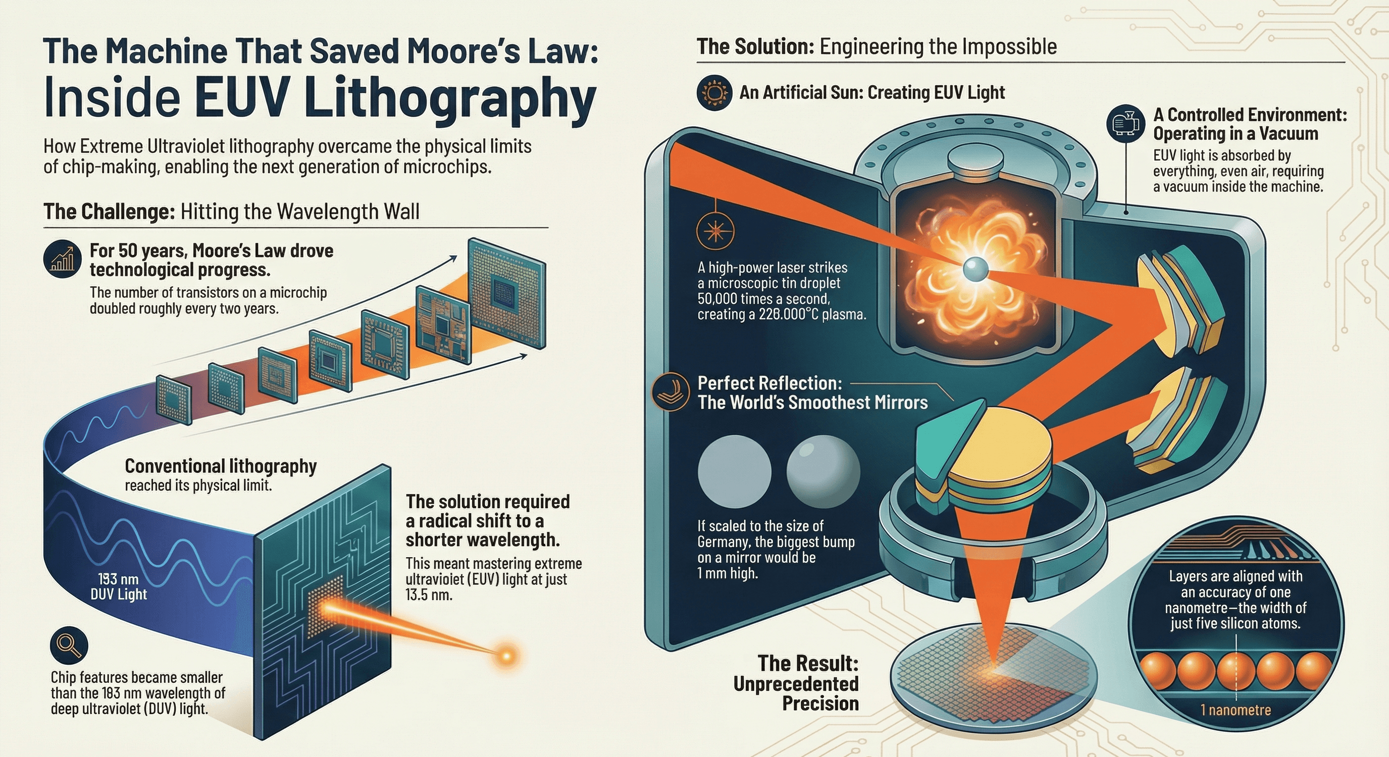
For decades, chip progress followed a simple rule: smaller transistors = more computing power
But there was a catch.
Chips are made by projecting light to draw circuit patterns. For years, the industry used deep ultraviolet (DUV) light.
Eventually, engineers hit a wall:
- The patterns they wanted were smaller than the wavelength of the light itself
- It’s like trying to draw fine pencil sketches using a thick paint roller
At that point, traditional lithography had reached its physical limit.
The Radical Idea
If the problem is that the light is too “large”…
Use much shorter light.
That’s where Extreme Ultraviolet (EUV) comes in:
- Wavelength: 13.5 nanometers
- That’s more than 10× smaller than previous technology
Sounds simple but here’s the twist:
EUV light is absorbed by almost everything.
- Air absorbs it
- Glass absorbs it
- Normal lenses are useless
So engineers had to reinvent chip manufacturing from scratch.
Creating an “Artificial Sun”
Since EUV light doesn’t exist naturally at usable levels, engineers had to manufacture it.
How?
- Fire a high-power laser at a microscopic molten tin droplet
- Do this 50,000 times per second
- The tin explodes into an extremely hot plasma
- That plasma emits EUV light
So we can say that the modern chips are made using tiny controlled explosions.
The World’s Smoothest Mirrors
Because EUV light can’t pass through lenses, the entire system uses mirrors instead.
But not ordinary mirrors:
- They’re made of dozens of atomic-scale layers
- Each mirror is polished so smooth that:
If scaled to the size of a country, the biggest bump would be just a millimeter high.
Even then, each mirror only reflects about 70% of the light. So engineers needed insane precision and power to make it work.
Working in a Vacuum
Since EUV is absorbed by air:
- The entire machine operates in a vacuum
- Even tiny dust particles can ruin a chip pattern
Everything - light generation, reflection, patterning happens in a sealed, controlled environment.
The Result
This is what EUV enables:
- Printing extremely tiny patterns in a single step
- Fewer manufacturing steps
- Fewer defects
- Much higher precision
Which is why today we can build:
- 7 nm, 5 nm, even 3 nm chips
- With billions of transistors
- Powering phones, AI models, data centers, and supercomputers
Why This Matters
EUV lithography isn’t just a better machine.
It’s:
- Physics pushed to its limits
- Engineering that borders on unreasonable
- One of the most complex systems humans have ever built
And without it, modern computing simply wouldn’t exist.
Next time you hear “3 nm chip”, remember:
It took lasers, plasma, mirrors smoother than reality, and a vacuum just to draw those lines.
What Comes After This?
Even EUV is approaching its own limits. To continue scaling beyond 2 nm, the industry is now deploying High-NA EUV; a new generation of machines with even higher optical precision and even tighter tolerances.
It is the same philosophy taken further: fewer tricks, more physics, and machines that push even closer to the edge of what reality allows.
Summary
EUV lithography is the near-impossible machine that turned atomic-scale physics into a manufacturable process, keeping Moore’s Law alive when everything else failed.
What makes EUV truly remarkable isn’t just that it works. It’s that it works reliably, repeatedly, and at global manufacturing scale.
This machine operates at the intersection of multiple extremes: extreme heat to generate the light, extreme cold and vacuum to preserve it, extreme smoothness to guide it, and extreme precision to place billions of features exactly where they belong. Every part of the system pushes against known physical limits, yet the whole operates as a single coordinated instrument.
EUV also represents a philosophical shift in engineering. Instead of clever shortcuts or incremental tricks, the industry chose to confront physics head-on, accepting inefficiency, complexity, and cost in exchange for correctness. When multi-patterning and software-driven fixes began collapsing under their own weight, EUV replaced workaround-heavy processes with a fundamentally cleaner solution: use the right wavelength, no matter how hard it is to tame.
Today’s most advanced chips: powering AI models, scientific simulations, smartphones, and data centers; are not just products of better design, but of this extraordinary manufacturing leap. Every transistor etched at 3 nm is a quiet proof that ideas once labeled “impractical” or “physically impossible” can still reshape the world when engineering ambition is allowed to outrun caution.
EUV lithography is not merely a tool in the semiconductor roadmap.
It is a reminder that progress doesn’t always come from elegance. Sometimes, it comes from building something so unreasonable that reality eventually has no choice but to cooperate.